Firefly PCB is a unique type of HDI PCB (High-Density Interconnect PCB). HDI PCB refers to a high-density interconnect printed circuit board, which revolutionizes the way circuit boards are utilized. It enables compact and intricate designs, making it ideal for tiny electronics. As devices like smartphones, smartwatches, and foldable screens continue to advance, Firefly PCB plays a crucial role in ensuring they function efficiently in smaller, more compact sizes.
The demand for HDI PCBs is rising as consumers seek portable and intelligent devices. Companies rely on HDI PCB technology to enhance circuit performance while maximizing space efficiency. With the rapid expansion of 5G technology, Firefly PCB has become essential in developing small yet powerful gadgets that meet the needs of modern technology.
Key Takeaways
Firefly PCB changes electronics with its small HDI design. It works great for tiny devices like phones and smartwatches.
Cool features like tiny holes and bendy materials help Firefly PCB work well while saving space and weight.
Firefly PCB works in tough places, making it a good pick for cars, hospitals, and airplanes.
The tech moves data quickly and keeps signals strong, which is important for things like smart gadgets and fast computers.
Using Firefly PCB can make products better, save time, and meet the need for new tech.
What Makes Firefly PCB HDI PCB Unique?
Core Features of Firefly PCB
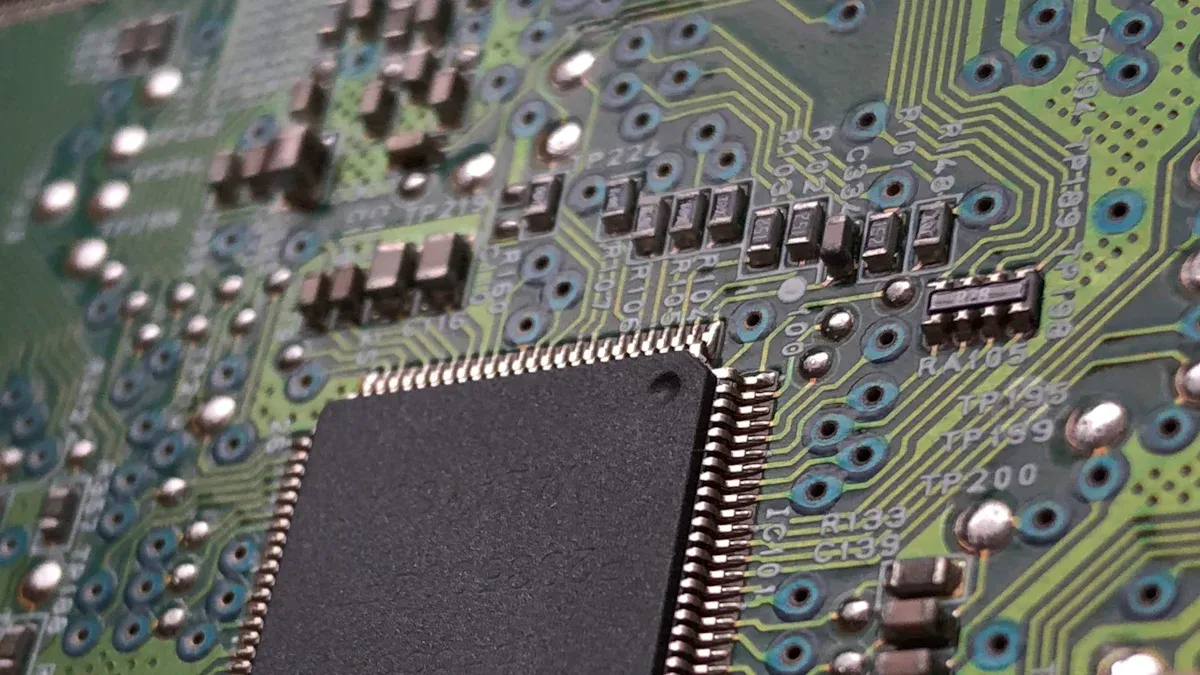
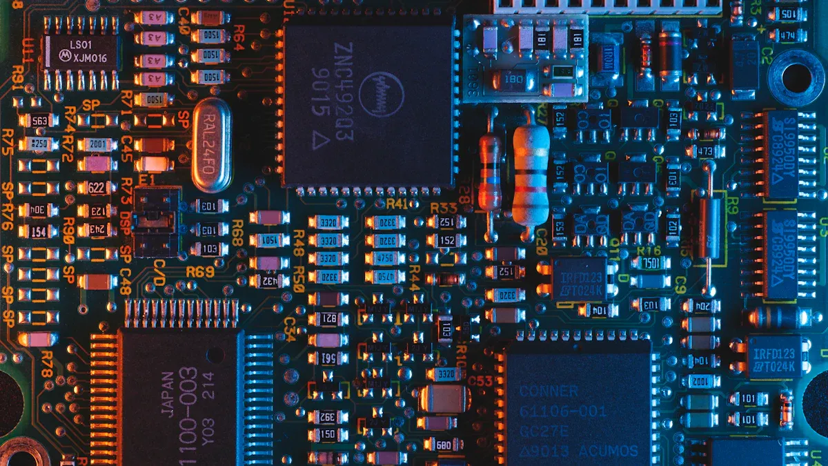
Firefly PCB HDI PCB is special because of its advanced features. It uses microvias, which are tiny holes that connect layers. These help make smaller devices without losing performance. Blind and buried vias are also used to handle complex circuits while staying thin.
The materials used in Firefly PCB are top-notch. They allow fast signal transfer and manage heat well. This keeps devices working great even in tough conditions. Its design supports many layers, making it perfect for small spaces needing high functionality.
Benefits in HDI and Flexible PCB Solutions
Firefly PCB offers benefits that regular PCBs can’t match. Its high-density design fits more parts into smaller spaces. This is important for gadgets like smartphones and wearables. Smaller designs save space and make devices lighter and easier to carry.
Firefly PCB is also great for flexible designs. It can bend or fold, which is useful for modern gadgets. Foldable phones and curved screens use this flexibility for better user experiences. Its strong electrical performance keeps signals clear, even in tight or bendable setups.
Firefly PCB is very durable too. It handles temperature changes and humidity better than regular PCBs. This makes it a favorite for industries like cars and airplanes, where conditions can be harsh.
Comparison with Traditional PCB Technologies
Firefly PCB beats regular PCBs in many ways. It provides better signal quality and less signal loss, especially for fast data. For example, its flyover cables lose less signal than normal PCB traces. This makes it great for high-speed data needs.
Firefly PCB also works well in different temperatures and humidity. Regular PCBs often fail in such conditions. Firefly PCB’s materials and methods ensure it stays reliable, even in tough environments.
Here’s a simple comparison of Firefly PCB and regular PCBs:
Feature | Firefly PCB HDI PCB | Traditional PCB |
|---|---|---|
Signal Quality | Excellent | Average |
Signal Loss | Low | High |
Stability in Conditions | Great | Okay |
Design Flexibility | High (uses microvias) | Limited |
Choosing Firefly PCB helps you make better, stronger, and smarter devices.
Firefly PCB’s Role in HDI PCB Technology
Microvias, Blind Vias, and Buried Vias
Firefly PCB HDI PCB is special because of its tiny holes. These include microvias, blind vias, and buried vias. Microvias are small holes that link PCB layers. They help make boards smaller but still work well. Blind vias connect the outer layer to an inner one. They don’t go through the whole board. Buried vias only link inner layers and stay hidden.
These features improve how well the board works. They reduce signal problems and make designs more reliable. They also let you fit more parts into less space. This is great for small devices like smartwatches and phones. Firefly PCB uses these smart techniques to meet modern tech needs.
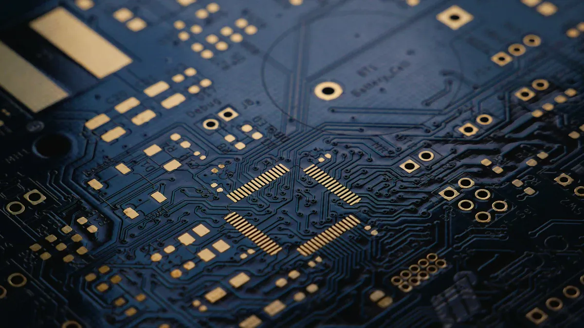
Advanced Stack-Up Designs
Firefly PCB uses smart layer designs to save space. A stack-up is how PCB layers are arranged. Firefly PCB’s stack-ups use copper and insulating layers. This helps balance size and performance.
These designs keep signals fast and clear. They also stop interference from messing up signals. Good stack-ups help manage heat, so devices stay cool. Whether for phones or cars, Firefly PCB’s designs fit your needs.
Material Innovations for HDI Applications
Firefly PCB uses top materials to make better boards. These include strong laminates and copper foils. They help with heat and keep boards working well. This is important for devices in tough conditions.
Firefly PCB also uses materials for flexible designs. This lets you make foldable gadgets without losing quality. These materials handle high-density needs for modern electronics. Firefly PCB ensures your designs are reliable and efficient.
Technological Advancements in Firefly PCB
Innovations in Manufacturing Processes
Firefly PCB has changed the hdi manufacturing process with new methods. It uses a firefly-inspired algorithm to improve production steps. This makes hdi pcb design more precise and efficient for modern devices. Automation, like better pick-and-place machines, speeds up production. These updates follow Industry 4.0 ideas, moving toward fully automated factories.
Title | Authors | Year | Summary |
|---|---|---|---|
Firefly-inspired algorithm for discrete optimization problems: an application to manufacturing cell formation | Sayadi MK, Hafezalkotob A, Naini SGJ | 2013 | Shows how a firefly-inspired algorithm improves manufacturing for Firefly PCB. |
Manipulation order optimization in industrial pick-and-place operations: application to textile and leather industry | N/A | 2024 | Explains how automation boosts production efficiency, helping Firefly PCB’s hdi manufacturing process. |
These improvements make production faster and keep the product strong. Firefly PCB leads in hdi technology with these advancements.
Enhanced Performance in Compact Designs
Firefly PCB delivers great electrical performance in small designs. Its hdi pcb layout allows fast data transfer and saves energy. For example, the Firefly Micro Flyover System reaches speeds of 56 Gbps PAM4 per channel. It uses little energy and fits into tiny spaces, making it perfect for high-tech uses.
Feature | Specification |
|---|---|
Data Rate | Supports up to 56 Gbps PAM4 |
Footprint | 0.63 in² for 265 Gbps/in² density |
Connector Size | 11.25 x 21.08 mm |
Application Areas | AI, high-performance computing, medical, test & measurement, FPGA |
With microvias and advanced materials, Firefly PCB keeps high-density interconnects reliable in small devices. This makes it a top choice for high density pcb needs.
Contributions to IoT and Wearable Devices
IoT and wearables need hdi pcb design for small, flexible gadgets. Firefly PCB provides printed circuit boards with strong interconnect abilities. It handles fast data and keeps signal integrity, perfect for smartwatches and fitness trackers.
The Firefly Micro Flyover System supports speeds up to 28 Gbps.
It uses both optical and copper interconnects.
Its small size fits well in wearable devices.
These features help create powerful, portable gadgets. Firefly PCB supports IoT and wearables, showing its focus on future hdi technology.
Applications of Firefly PCB Across Industries
Consumer Electronics: Smartphones and Wearables
Firefly PCB is important for today’s electronics. Smartphones and wearables help you stay connected and healthy. These gadgets need to be small and work well. Firefly PCB’s smart design fits more parts into tiny spaces. Its microvias make fast data transfer possible.
Foldable phones and curved screens need flexible boards. Firefly PCB uses materials that bend without losing performance. This makes devices better to use and keeps signals strong. From smartwatches to smartphones, Firefly PCB makes gadgets light, tough, and efficient.
Automotive: ADAS and Electric Vehicles
Cars use Firefly PCB for systems like ADAS and electric vehicles. These systems need small, powerful circuit boards. Firefly PCB’s design connects sensors, cameras, and processors reliably.
Firefly PCB handles heat and vibration well, which are common in cars. Its strong materials and smart production make it last in tough conditions. Whether it’s an electric car or safety tech, Firefly PCB helps your car work better.
Healthcare: Medical Devices and Diagnostics
Medical tools need to be accurate and dependable. Firefly PCB provides both with its advanced designs. Portable health monitors and diagnostic tools work faster with Firefly PCB. Its design processes data quickly for accurate results.
Firefly PCB materials survive cleaning and tough conditions. Flexible boards allow creative designs like bendable health sensors. With Firefly PCB, medical devices become better, easier to carry, and more reliable for patient care.
Aerospace: Lightweight and Strong Systems
In aerospace, weight is very important. Lighter parts help planes and spacecraft work better. Firefly PCB makes special circuit boards for high-performance systems. Its smart designs and materials are great for aerospace needs.
Firefly PCB uses advanced HDI technology to make small boards. These boards are light but still work well. Microvias and stack-up designs fit many layers into tiny spaces. This saves room while keeping connections strong.
Aerospace tools need to handle tough conditions. Firefly PCB works in high heat and strong vibrations. Its sturdy materials last a long time, even in hard environments. It’s perfect for navigation, communication, and control systems.
Modern aerospace designs need flexible parts. Firefly PCB can bend or curve for new ideas. This helps make foldable or curved components for planes and spacecraft.
Firefly PCB gives you lightweight, strong, and reliable boards. It helps you create new aerospace designs that meet strict rules.
The Future of Firefly PCB in 2025
Trends in HDI and Flexible PCB Technology
HDI technology is growing as devices get smaller and smarter. In electronics, HDI helps make tiny gadgets like phones and tablets. Wearable tech, like fitness bands and smartwatches, uses HDI to stay small but useful. Cars also use HDI to improve safety and control systems. These changes show how HDI is shaping the future of many industries.
Challenges and Opportunities
HDI technology has great potential but also some problems. Making HDI PCBs costs a lot because of special materials and steps. Engineers find it hard to design HDI layouts since they are complex. But these problems bring chances to improve. Companies can create better tools to lower costs and boost performance. Expanding to new markets and using eco-friendly methods can also help businesses grow.
Invest in research to create better HDI designs.
Find new markets to reach more customers.
Use green methods to meet eco-friendly demands.
Firefly PCB’s Role in Shaping the Future
Firefly PCB is ready to lead in HDI technology. Its advanced process makes precise and efficient PCBs for many industries. Firefly PCB’s smart materials and designs keep connections strong in small devices. By focusing on green practices and flexible layouts, Firefly PCB is building the future of electronics. Whether for wearables or cars, Firefly PCB helps you create amazing products.
Firefly PCB has changed how we make dense and flexible circuits. Its smart features help create smaller and better devices for healthcare, cars, and planes. By leading new ideas, it helps your products stay modern. As 2025 nears, Firefly PCB stands out in shaping future electronics. Its skill to follow new trends makes it key for your next big designs.
FAQ
What is Firefly PCB, and how is it different from regular PCBs?
Firefly PCB is a special kind of HDI PCB. It is made for small and flexible gadgets. Unlike regular PCBs, it uses tiny holes like microvias to save space. Its strong materials make devices lighter, smaller, and long-lasting.
Why is Firefly PCB useful for wearable gadgets?
Wearable gadgets need small and bendable circuit boards. Firefly PCB is perfect for this because it is flexible and compact. It works well in small spaces, making it great for smartwatches and fitness bands.
Can Firefly PCB survive tough conditions?
Yes, Firefly PCB is made to handle hard environments. It can resist heat, moisture, and shaking. This makes it great for cars, planes, and medical tools where strength is important.
How does Firefly PCB help the environment?
Firefly PCB helps by using smart materials and less waste. Its small designs use fewer resources, and its strength makes products last longer. This supports eco-friendly goals in making electronics.
Which industries use Firefly PCB the most?
Firefly PCB is used in many industries like electronics, cars, and healthcare. It powers phones, wearables, electric cars, medical tools, and airplane systems. Its flexibility and strength make it useful everywhere.
See Also
Emerging Trends in Smart Manufacturing for PCBA by 2025
Simplifying Flex and Rigid-Flex PCBA Manufacturing Processes
Key Trends Influencing Industrial IoT PCB Assembly for 2025
Navigating ITAR Compliance in PCBA Manufacturing for 2025
Essential Technologies Transforming PCBA Manufacturing in Consumer Electronics