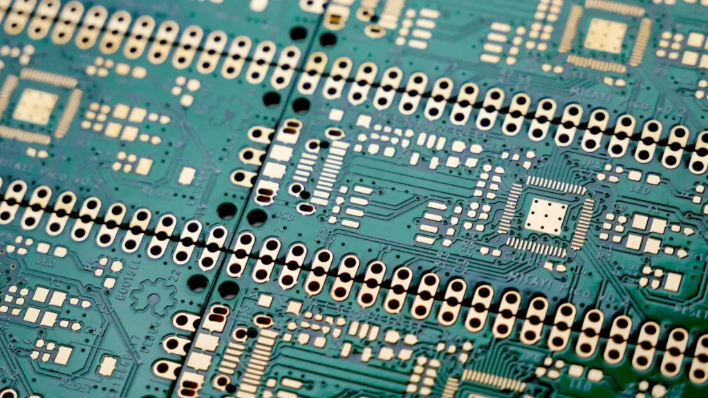

High-Density Interconnect (HDI) PCBA technology is a big step forward in electronics. Unlike regular circuit boards, HDI uses smart designs to fit more parts and work better. This helps make devices smaller, faster, and more efficient, meeting the need for tiny gadgets in today’s world.
The global HDI PCB market is expected to grow from $9.1 billion in 2024 to $13.9 billion by 2033. This growth is due to trends like 5G, IoT, and new car technologies. It shows how important HDI is for the future of electronic designs.
HDI PCBs are key for industries needing small, reliable, and fast devices. They improve signal quality and save space, making them vital for advanced technology.
Key Takeaways
HDI PCBs are small and fit more parts in less space. This is important for devices like phones and medical tools.
HDI PCBs work better by reducing signal problems and speeding up data. They are great for fast systems like telecom and airplanes.
HDI PCBs are strong and made with methods that lower mistakes. This makes them reliable for cars and defense equipment.
HDI technology costs more at first but saves money later. It cuts down on errors and uses fewer materials.
More people want HDI PCBs because of 5G, IoT, and smart cars. These trends show how useful they are for future electronics.
Key Features and Benefits of High-Density Interconnect (HDI) PCBA
Compact Design and Space Efficiency
HDI technology changes how we use space in electronics. It allows more parts to fit into smaller spaces. This is important for modern gadgets that need to save space.
Mobile Devices: HDI helps make thinner, smarter phones by fitting more circuits.
Automotive Electronics: Cars use HDI for compact systems like smart driving tools.
Medical Devices: Small health gadgets work well with HDI’s space-saving designs.
5G Infrastructure: HDI supports fast 5G networks while staying small in size.
HDI PCBs also need fewer layers, making designs more flexible. Engineers can create lighter, efficient products without losing quality.
Improved Electrical Performance
HDI PCBs work better electrically, making them great for advanced uses. They keep signals strong by placing parts closer together. This reduces signal loss and ensures smooth data flow.
Special via-in-pad design helps with heat and electricity flow.
Shorter connections lower signal problems and improve performance.
Smaller boards with more transistors use less power but stay fast.
These features make HDI PCBs perfect for industries like telecom and aerospace that need strong electrical systems.
Enhanced Reliability and Durability
HDI PCBs are built to last and handle tough conditions. Their small design lowers the chance of errors, and advanced methods make them stronger.
Using micro vias and buried vias makes HDI PCBs sturdier than older designs. This reduces noise and keeps signals clear. They also manage heat well, working steadily even when hot.
These traits make HDI PCBs a trusted choice for fields like aerospace, cars, and medical tools, where strength is crucial.
Cost-effectiveness in production
At first, HDI might seem expensive. However, its long-term benefits save money for many industries.
One reason HDI saves money is by reducing mistakes. Errors in making boards can cost a lot to fix. HDI lowers these risks with better control of spacing and widths. This accuracy means fewer problems, saving time and money.
HDI PCBs need fewer layers because they use space well. Fewer layers mean less material and easier production.
Micro-vias and advanced techniques make HDI PCBs more reliable. This reduces the need for repairs or replacements.
Better production results with HDI lead to fewer defects. This improves quality and saves costs.
Designing HDI PCBs costs more at first, about 2-4 times higher than regular boards. But this extra cost is worth it. The accuracy and strength of HDI designs prevent costly mistakes later. For industries like aerospace or medical tools, this is very important.
Tip: Spending more on HDI now can save money later. It avoids errors and cuts material waste.
HDI PCBs also help make electronics smaller. Compact designs need fewer parts and smaller cases. This lowers production costs even more. HDI is a smart choice for making high-quality, affordable products.
Applications of HDI PCBs in Modern Industries
Consumer Electronics
HDI is important for making small, powerful gadgets. Devices like phones, laptops, and tablets use HDI to stay slim and work well. HDI helps fit more features into smaller devices without losing quality.
More people want HDI PCBs for their electronics.
Smaller, faster gadgets are driving this demand.
Examples include smartwatches, gaming systems, and home tech.
HDI improves how devices work while keeping them light and easy to carry. This makes HDI a key part of today’s electronics.
Automotive Systems
Cars now use HDI PCBs for advanced systems. Features like smart driving tools, electric cars, and entertainment systems need HDI to work.
Evidence Type | Details |
|---|---|
Growing Demand | More cars need HDI PCBs for smart systems and EVs. |
Smaller Designs | Tiny parts and faster data push HDI use in cars. |
Better Features | Layers, materials, and built-in parts improve how HDI works in vehicles. |
New Trends | AI, machine learning, and new materials shape HDI in cars. |
HDI makes car systems smaller and stronger for tough conditions. It also helps add AI and smart tech to vehicles.
Telecommunications
Telecom depends on HDI PCBs for fast data and small designs. With 5G growing, HDI ensures quick and steady communication.
HDI PCBs keep signals strong and data flowing smoothly.
They help make smaller network tools.
Used in routers, switches, and signal stations.
HDI PCBs help telecom provide better connections and handle more data. This makes HDI essential for modern communication.
Medical devices
HDI technology is very important for improving medical devices. These devices help doctors diagnose and treat patients better. HDI PCBs make small, powerful tools that meet healthcare needs today.
Medical devices use HDI to fit more circuits and keep signals clear. This helps them work well, even in serious situations. For instance, HDI lowers electromagnetic interference. This is crucial for keeping devices like pacemakers and imaging machines accurate.
Why HDI is Great for Medical Devices:
More circuits mean smaller devices with more features.
Clear signals help send data correctly.
Less interference makes devices more dependable.
Smaller designs allow wearable and portable gadgets.
HDI also helps create new tools like robotic surgery systems and advanced scanners. These tools need strong and precise circuit boards to work right. With HDI, companies can make medical devices that are smaller, stronger, and more efficient.
Aerospace and defense
HDI PCBs are very important in aerospace and defense. These fields need safe and reliable systems, and HDI helps them work perfectly. The technology handles fast signals and tricky designs, making it great for critical tasks.
The 10+ layers HDI type is especially useful in aerospace and defense. It offers top performance, dependability, and compact designs for systems like communication and control.
Type | Use Area | Main Benefits |
|---|---|---|
10+ Layers HDI | Aerospace and Defense | Top performance, dependability, and small size |
General HDI PCBs | Communication and Control Systems | Combines many functions into one board |
HDI lets many functions fit into one PCB. This makes equipment smaller and lighter, which is key for aerospace. For example, satellites and planes use HDI for fast data and steady performance in tough conditions.
The need for HDI in aerospace and defense is growing. You can see its role in radar systems, navigation tools, and secure communication networks. HDI keeps these systems working well, even in hard environments.
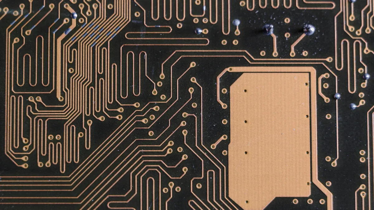
Types of Vias in High-Density Interconnect PCBs
Micro-vias and their importance
Micro-vias are tiny holes used in HDI PCBs. They are smaller than 150 micrometers and connect PCB layers. Their small size helps make compact and advanced designs. This is important for devices needing many features in small spaces.
Micro-vias are made using lasers, plasma, or chemicals. These methods are precise and avoid heat damage. The depth-to-width ratio of micro-vias is very important. Keeping this ratio correct makes them reliable. Stacked micro-vias improve signals and reduce interference in fast circuits.
Copper is often used in micro-vias. It helps electricity flow and manages heat well. This makes micro-vias very useful for HDI PCBs in industries like telecom and aerospace.
Blind and buried vias
Blind and buried vias are key for HDI PCB designs. Blind vias connect one inner layer to an outer layer. Buried vias link two or more inner layers without reaching the surface. These vias save space by avoiding through-holes, which limit design options.
Feature | Blind Vias | Buried Vias |
|---|---|---|
Connectivity | Link an inner layer to ONE outer layer | Link two or more inner layers only |
Penetration | Partially go through the PCB stackup | Fully go through the layers they join |
Inspection | One opening allows visual checks | No visual checks or probe test points |
Manufacturing | Needs careful depth control | Needs very tight layer alignment |
Blind and buried vias help HDI PCBs handle complex designs. They are great for uses where space and signal quality matter most.
Via-in-pad method
The via-in-pad method is a big improvement for HDI PCBs. It places vias directly in component pads, saving space and boosting performance. Shorter signal paths lower unwanted effects, which is vital for fast circuits.
This method also helps manage heat better. Vias in pads let heat escape quickly, perfect for high-power devices. It also allows tighter layouts, making PCBs smaller overall.
Tests like temperature cycling and strength checks prove this method works well. It ensures strong soldering and steady performance, even in tough conditions. The via-in-pad method is popular in telecom and medical devices, where small and powerful designs are needed.
Manufacturing Process of HDI PCBs
Design and Layout
The design phase is the first step in making HDI PCBs. You need to plan where parts, traces, and vias will go. This helps the board work well and be easy to make. HDI designs use advanced methods to save space and improve performance.
Aspect | Description |
|---|---|
Via Types | Uses blind, buried, and micro vias for better routing. |
Layer Stackup | Decides layer order and materials, affecting signals and paths. |
Design Rules | Sets limits for trace width, via size, and spacing. |
DFM Guidelines | Includes trace sizes, ring specs, and impedance control. |
Routing Efficiency | Depends on stackup, via types, and part placement. |
The stackup is very important in HDI PCB design. It shows how layers connect and affects how well the board works. Following design rules helps avoid mistakes and ensures the board meets standards.
Layering and Lamination
Layering and lamination build the HDI PCB’s structure. Layers are stacked and pressed together to form one solid board. Each layer must line up perfectly for accuracy. Heat and pressure bond the layers, making the board strong and reliable.
Materials must handle high-speed signals and heat well. The layering process ensures the board can manage complex designs and stay sturdy. Good lamination stops layers from peeling apart and keeps the board durable in tough conditions.
Drilling and Plating
Drilling and plating are key steps in making HDI PCBs. Drilling makes vias that link the board’s layers. Laser drilling is used for tiny micro vias because it is very precise.
To get good results, follow these tips:
Match drill sizes to part leads and keep proper spacing.
Use a 10:1 ratio for through holes to avoid plating issues.
Laser drill holes smaller than 0.15 mm for accuracy.
Keep hole positions within ±0.05 mm for precision.
Ensure even plating to prevent electrical problems.
Plating adds a thin copper layer inside the drilled holes. This improves conductivity and strengthens layer connections. Proper depth control of blind and buried vias ensures the board works well for advanced uses.
Testing and Quality Assurance
Testing ensures HDI PCBs work well and meet high standards. Every part of the board must be checked carefully. This process has many steps to find problems early.
One important step is creating test fixtures. These tools must match electrical needs and layout rules. Good test fixtures give accurate and reliable results. Another step is de-embedding, which removes unwanted effects from tests. Using a library of tested S-parameters keeps results consistent. Checking S-parameter quality is also very important. A set process ensures artefacts stay within safe limits for good signals.
Area | Solution |
|---|---|
Test fixture design | Structures must meet electrical needs and layout rules. |
De-embedding | Use tested S-parameters for consistent results across tools. |
S-parameter quality | Follow steps to check artefacts stay within safe limits. |
Functional testing checks if the HDI PCB works as planned. This includes testing signals, power flow, and heat control. Tools like automated optical inspection (AOI) and X-ray inspection find problems like bad vias or solder joints. These methods ensure the board meets top quality standards.
Focusing on testing lowers failure risks and boosts reliability. This is very important for fields like aerospace, telecom, and medical devices, where accuracy and strength are critical.
High-Density Interconnect PCBs vs. Conventional PCBs
Structural Differences
HDI PCBs are built for advanced technology. They use microvias, blind vias, and buried vias. These are tiny holes made with lasers for precision. Regular PCBs use through-hole vias, which are bigger and drilled mechanically.
Feature | HDI PCB | Standard PCB |
|---|---|---|
Trace Density | High – fits fine lines and tight spaces | Moderate – fewer routing options |
Via Types | Microvias, blind/buried vias – small and laser-drilled | Through-hole vias – larger and drilled mechanically |
Layer Count | Often 8+ layers – compact and dense layouts | 2–6 layers – basic designs |
HDI PCBs use thin cores for better performance and compact size. These cores need careful handling during production. Special methods like pulse-spray technology help process blind vias and small features accurately. These improvements allow HDI PCBs to pack more functions into smaller spaces, making them great for high-tech devices.
Performance Comparison
HDI PCBs work better than regular PCBs in many ways. Their small traces and vias allow more parts in less space. For example, HDI PCBs have trace widths under 100 microns. This helps make smaller gadgets without losing features.
Shorter signal paths in HDI PCBs reduce noise and improve data flow. This makes them perfect for fast and complex designs. HDI PCBs also handle heat better. They use more copper to spread heat evenly, keeping devices reliable in tough conditions.
Regular PCBs have bigger traces and through-hole vias, which limit their design options. They are fine for simple uses but can’t match HDI PCBs in speed or advanced designs. HDI PCBs are ideal for things like smartphones, medical tools, and fast communication systems.
Cost and Complexity
Making HDI PCBs costs more and takes longer than regular PCBs. HDI PCBs need special processes like laser drilling and multi-layer lamination. These steps add time and expense.
Feature | Standard PCB | HDI PCB |
|---|---|---|
Cost | Lower | Higher |
Layer Count | 1–16 layers | Often 8+ layers |
Feature Size | Larger traces and spaces | Smaller traces and spaces, microvias |
Via Technology | Through-hole vias | Microvias, blind vias, buried vias |
Density | Lower component density | Higher component density |
Performance | Basic applications | Great for fast and complex designs |
Manufacturing Complexity | Simple process | Advanced process, multi-layer lamination |
Turnaround Time | Shorter | Longer |
Typical Cost Per Board | 0.5–5 USD | 3–30 USD |
HDI PCBs cost more because they use better materials and smaller features. Microvias and blind vias make production harder. Aligning layers and adding advanced finishes also raise costs.
Even though HDI PCBs are pricey upfront, they save money later. Their strong design means fewer repairs and replacements. For industries like aerospace and healthcare, where accuracy matters, HDI PCBs are worth the investment.
Tip: Spending more on HDI PCBs now can save money later. Their advanced features and reliability make them a smart choice for high-tech devices.
HDI technology is key for making modern electronics smaller and better. It works better than regular PCBs by saving space and improving performance. New fields like defense and space use HDI for fast data and processing. The global PCB market is growing fast because people want smarter phones and gadgets. As technology changes, HDI will lead the way with its amazing features.
FAQ
How are HDI PCBs different from regular PCBs?
HDI PCBs use special features like microvias and blind vias. These help fit more parts and improve performance. Regular PCBs use through-hole vias, which take up more space. HDI PCBs are better for modern, advanced gadgets.
Why are microvias important in HDI PCBs?
Microvias link layers in HDI PCBs while saving space. Their tiny size keeps signals clear and reduces problems. This makes them perfect for small, powerful devices like phones and medical tools.
Are HDI PCBs more costly to make?
Yes, HDI PCBs cost more because of advanced processes like laser drilling. But they last longer and work better, saving money over time. This is great for industries needing strong and precise boards.
Can HDI PCBs handle fast signals?
Yes! HDI PCBs are great for fast signals. Their short paths and exact designs reduce noise and keep data flowing smoothly. They are ideal for telecom, aerospace, and other advanced uses.
Which industries use HDI PCBs the most?
Industries like electronics, cars, telecom, medical tools, and aerospace use HDI PCBs. These fields need small, reliable, and high-performing solutions, which HDI provides well.
See Also
Understanding Mixed Technology in PCBA Production Processes
Expert Techniques for Achieving Superior PCBA Manufacturing
Innovations in RSJPCBA Design Through Artificial Intelligence