The growth of IoT devices necessitates improved methods for IoT device PCBA manufacturing. These devices are compact and require high performance. Traditional manufacturing techniques are no longer sufficient for them. For instance, the global PCB assembly market was valued at $22.5 billion in 2023 and is projected to expand at a rate of 6.1% annually, reaching $38.5 billion by 2032. This indicates that more industries, such as automotive and manufacturing, are adopting advanced electronics. Accurate PCBA manufacturing for IoT devices is crucial for their functionality and expansion, highlighting their significance in the Internet of Things.
Key Takeaways
Making IoT PCBA is key to building small, powerful devices for today’s tech needs.
Tiny parts and packed designs in IoT need smart ideas to work well and last long.
Good power use and heat control help IoT devices last longer and work better.
Careful part placement and strict checks stop mistakes and keep devices working well.
Using machines in PCB assembly speeds up making devices and keeps quality steady to meet rising demand.
Challenges in IoT PCB Assembly
The fast growth of IoT devices brings new problems for PCB assembly. These issues arise from needing small designs, strong performance, and reliability. Let’s look at the main challenges manufacturers face.
Miniaturization and Space Constraints
IoT devices are getting smaller and easier to carry. This requires new ways to fit circuits into tiny spaces. Miniaturization creates several problems:
Ultra-Compact Design: Methods like via-in-pad help fit more circuits and keep signals clear, making PCBs smaller.
Advanced SMT Methods: Placing parts carefully allows tight packing and good heat control.
Flexible PCBs: These bendable boards allow creative designs in small spaces, perfect for IoT devices.
Smaller designs make devices portable and save energy. But circuits must be separated to avoid signal problems. For example, keeping analog and power signals apart stops interference and keeps performance high.
High Component Density and Multi-layer Boards
IoT PCB assembly often uses many parts and multi-layer boards. These are needed to add sensors, power systems, and wireless features in small devices. But they also bring challenges:
Multi-layer PCBs are in high demand for compact, efficient designs. They allow dense connections, which are key for modern IoT devices.
Making multi-layer PCBs costs a lot. The special materials and steps needed make them pricey, which is tough for industries with tight budgets.
As devices shrink, microvias are now common in multi-layer PCBs. They improve connections and boost performance in small designs.
Even with these issues, advanced PCB technologies help IoT devices meet today’s needs.
Power Efficiency and Thermal Management
Power use and heat control are vital for IoT PCB reliability. These devices often work in places where heat and energy use are big concerns.
Good power strategies include special planes for power flow and energy-saving parts. These steps improve performance and make batteries last longer.
Heat control methods, like thermal vias and copper layers, remove heat well. Placing heat-making parts carefully also avoids hot spots.
Using heat simulations during design and adding temperature sensors improves reliability further.
By solving these problems, manufacturers ensure IoT devices work well and stay high-quality over time.
Importance of Advanced IoT PCBA Manufacturing
Precision in Component Placement
Placing parts accurately is key for IoT PCB success. As IoT devices get smaller, every bit of space matters. New assembly methods help place parts perfectly, avoiding errors and improving how devices work.
Did you know? Misplaced parts can cause big problems in IoT devices. Advanced tools in PCB assembly fix this by ensuring perfect placement.
The PCB market has changed to meet modern tech needs. For example, fast systems like 5G need PCBs that handle high speeds. Accurate part placement keeps signals strong and devices reliable.
Evidence | Description |
|---|---|
Precision in PCB Assembly | New tools ensure the accuracy needed for modern PCBs. |
Component Placement | Misplaced parts can cause failures, so precision is vital. |
Cost-Effectiveness | Better tools improve accuracy and save money during assembly. |
Using better materials and methods helps manufacturers make reliable and cost-friendly IoT devices.
Signal Integrity for High-speed Data Transmission
IoT devices need fast data transfer for their features to work well. Keeping signals clear is very important, especially for devices handling lots of data or working at high speeds.
To keep signals strong, advanced methods reduce interference and create clear paths. For example, separating analog and digital signals stops problems like cross-talk. Multi-layer PCBs with smart designs also keep signals steady in small devices.
Ways to keep signals clear include:
Using special traces to stop signal loss.
Adding ground planes to block interference.
Designing traces to avoid sharp bends or overlaps.
With more IoT devices and edge computing, special PCBs are in demand. By focusing on signal clarity, devices can work better and more reliably.
Quality Control for IoT Reliability
Good quality control ensures IoT devices work well. Without careful checks, small mistakes can ruin device performance. Advanced methods like Automated Optical Inspection (AOI) and X-ray checks find problems early.
Quality Control Method | Purpose |
|---|---|
Automated Optical Inspection (AOI) | Spots surface issues like misplaced parts or bad soldering. |
X-ray Inspection | Finds hidden problems like cracks or solder voids. |
In-Circuit Testing (ICT) | Tests if each part works correctly. |
These checks make sure PCBs meet high standards for IoT devices. For example, using heat sensors during design helps find and fix problems early. Strong quality control makes devices last longer and work better.
Pro Tip: Regular PCB tests can catch problems early, saving time and money.
Advanced IoT PCBA manufacturing solves size and part challenges while ensuring top quality and performance.
Benefits of Advanced IoT PCB Assembly

Stronger and Longer-lasting Devices
Advanced PCB assembly helps IoT devices handle daily use. These devices are important for many tasks, so they must last. Using high-quality materials and careful assembly makes PCBs work longer. For example, better soldering stops weak spots that might break later.
Managing heat is also key to making devices durable. Heat-resistant materials and smart cooling designs keep devices working well, even in tough conditions. This is crucial for devices with sensors that check temperature, pressure, or other factors in industries. When PCBs are built strong, IoT devices stay reliable.
Tip: Take care of your IoT devices to make them last longer.
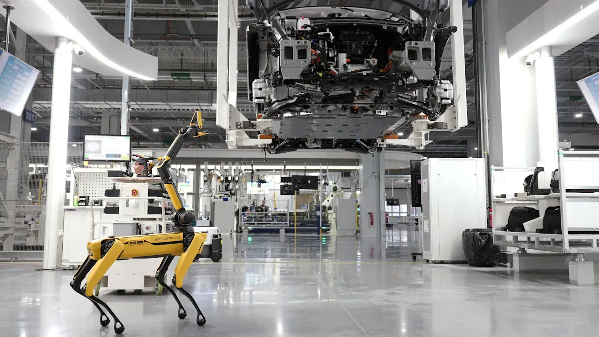
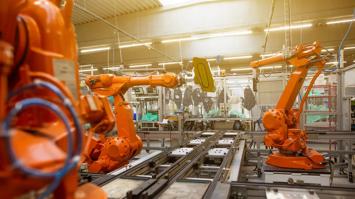
Easier Large-scale Production
Making many IoT devices quickly is important for growing markets. Advanced PCB assembly helps produce large amounts without losing quality. Automation has changed how factories work, cutting down on mistakes and saving time. This keeps every batch consistent.
For example, automated systems can now deliver stencils in just an hour. This speed helps factories adjust to demand changes fast. Whether you need a few devices or many, modern PCB assembly can handle it.
Feature | Description |
|---|---|
Factory Locations | Factories in Shenzhen and Huizhou meet different needs. |
Production Capacity | Handles both small and large production orders. |
Delivery Efficiency | Stencils delivered in 1 hour for faster production. |
These improvements make it easier to produce IoT devices in large numbers while keeping quality high.
Better Connectivity Features
IoT devices need strong connections to work well. Advanced PCB assembly adds features like Wi-Fi, Bluetooth, and 5G. These technologies keep devices connected to the cloud or other devices.
To support this, manufacturers use multi-layer PCBs with smart designs. These boards reduce interference and keep signals clear, even in small devices. Ground planes and special traces also help by stopping signal loss.
As IoT grows, better connectivity will be needed. Advanced PCB assembly ensures devices can handle these demands, keeping you connected in a fast-changing world.
Did you know? Multi-layer PCBs are key to adding advanced connectivity to IoT devices.
Modern IoT PCB assembly methods are crucial for IoT devices. These methods help devices work well, even with small sizes and many parts. They also improve connections, making devices run smoothly in today’s tech world.
IoT’s future relies on better manufacturing ideas. As technology grows, advanced PCBA methods will boost IoT’s performance and growth. These improvements will change how IoT devices link and work in the future.
FAQ
What does PCBA mean in IoT devices?
PCBA means Printed Circuit Board Assembly. It’s the process of putting electronic parts on a PCB. For IoT devices, PCBA makes sure all parts work together. This helps with connecting, processing data, and communicating.
Why is making IoT PCBs smaller important?
Smaller PCBs make IoT devices easy to carry and use. They fit into small spaces but still work well. This is very important for wearables, smart sensors, and tiny IoT gadgets.
How does advanced PCBA make IoT devices better?
Advanced PCBA uses special tools and checks for mistakes early. Tools like Automated Optical Inspection help place parts correctly. This makes sure IoT devices work well, even in tough conditions.
Why is heat control important for IoT PCBs?
Heat control stops parts from getting too hot and breaking. Things like thermal vias and heat-safe materials help remove heat. This keeps IoT devices safe and working for a long time.
What’s next for IoT PCB assembly?
Future IoT PCBs will use AI to design better boards. Flexible PCBs will allow cool new uses. New materials will save power. These changes will help make smarter and more connected devices.
See Also
Evaluating Top All-in-One PCBA Manufacturing Solutions for 2025
Discover The Role of AI in Advancing PCBA Technology
2025 Analysis: Turnkey PCBA Versus Consignment Production Methods
Achieving Superior Quality Through Effective PCBA Manufacturing Methods
Understanding Mixed Technology PCBA Manufacturing Processes and Benefits