1. Basic structure and typical applications
Range of layers
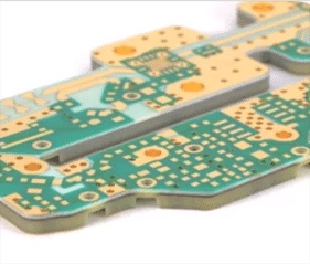
Usually 4~12 layers (higher layers can be more than 20 layers), through the lamination process to realize the alternating stack of insulating layers and conductive layers.
Example: The common structure of 6-layer board is Signal-GND-Power-Signal-GND-Signal.
Typical Application Scenarios
Low to medium speed digital circuits (e.g., industrial control motherboards, power supply modules);
Analog signal processing (such as audio amplifiers);
General consumer electronics (such as home appliance control boards, routers).
2. Material Characteristics Requirements
Substrate selection
FR-4 epoxy glass cloth: mainstream material, low cost, suitable for most scenarios (Tg=130~140℃).
High-frequency scenario: optional low-loss material (e.g. Isola 370HR, Dk=4.0, Df=0.02@1GHz).
Copper Foil Thickness
The outer layer is usually 1oz (35μm), the inner layer is 0.5~1oz, and can be locally thickened to 2oz for high current path.
3. Design Specifications and Process Requirements
Line design
Line width/spacing: 5~8mil (125~200μm) for conventional design, can be reduced to 3mil (75μm) for high precision.
Impedance control: ±10% tolerance (e.g. 50Ω single-ended, 100Ω differential) to be realized by stacking design.
Drilling and Hole Metallization
Mechanical drilling: hole diameter ≥ 0.3mm (12mil), depth to diameter ratio of ≤ 10:1 (e.g. 0.3mm hole diameter corresponds to 3mm plate thickness).
Copper plating thickness: hole wall copper thickness ≥20μm, to ensure mechanical strength and electrical conductivity.
Interlayer alignment: Interlayer offset ≤ 50μm (to be calibrated by optical positioning system).
4. Key process steps
Lamination process
Alternate stacking of prepreg and copper foil, high temperature and high pressure curing (180~200℃).
Thickness tolerance (±10%) after lamination needs to be controlled.
Surface treatment
Spray tin (HASL): low cost, but poor flatness, suitable for large pitch components.
Immersion gold (ENIG): high flatness, suitable for BGA / SMD welding, but need to prevent “black disk” problem.
OSP (organic protective film): low-cost program for short storage cycles.
5. Reliability test standards
Thermal Reliability
Thermal cycle test (-40℃~125℃, no delamination after 500 cycles).
Soldering heat resistance test (260°C, 10 seconds, no blistering after 3 cycles).
Mechanical Reliability
Peel strength test (≥1.0N/mm, IPC-TM-650 2.4.8)
Vibration test (e.g. 20G RMS, 3 axes, 2 hours per axis without failure).


Valoraciones
No hay valoraciones aún.