
The Photo-Sensitive Layer, or PSL, is important in PCB making, especially in sustainable PCBA manufacturing. It helps create accurate circuit designs for small and smart devices. In flexible PCBs, PSL makes them bendable but still strong. It also helps save materials and supports eco-friendly methods. By 2025, PCB makers will use new ideas to save energy and cut waste. These changes help protect the environment.
Key Takeaways
PSL means Photo-Sensitive Layer, important for making precise PCB designs.
Flexible PCBs use PSL to stay bendable but strong for new devices.
PSL helps save materials and supports green manufacturing in the PCB field.
It improves how long flexible PCBs last and work, perfect for smartwatches.
PCB makers now focus on saving energy and cutting waste, with PSL helping a lot.
What is PSL in the PCB Industry?
Definition and Full Form of PSL
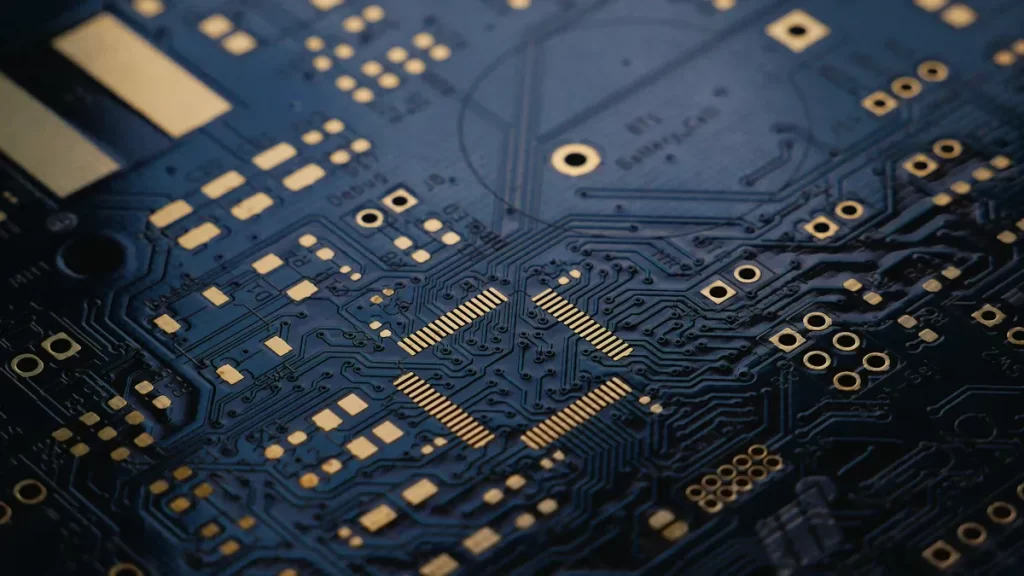
PSL means Photo-Sensitive Layer. It is a special coating used to make printed circuit boards (PCBs). This layer changes when exposed to light during production. It helps create exact patterns on the PCB’s surface. PSL ensures the circuit design is copied correctly onto the board. This is very important for modern electronics, where small size and accuracy matter.
The Photo-Sensitive Layer is especially useful for making flexible PCBs. It helps create detailed designs while keeping the board bendable. This makes it essential for advanced devices like smartwatches and foldable screens.
Importance of PSL in PCB Manufacturing
The Photo-Sensitive Layer is crucial in making PCBs. It improves the accuracy of circuit designs, which helps devices work better. Using PSL, manufacturers can make high-quality boards with fewer mistakes. This saves time, materials, and effort.
PSL also helps make flexible PCBs. These are used where regular stiff boards don’t work well. For example, flexible PCBs are found in medical tools, cars, and gadgets. PSL ensures these boards are strong and reliable.
PSL also supports eco-friendly manufacturing. It reduces waste during production. This matches the growing focus on sustainability in the electronics industry.
Key Features of PSL in Modern PCB Applications
The Photo-Sensitive Layer has many features that make it important for today’s PCBs:
High Precision: PSL helps create detailed and exact circuit patterns. This is needed for advanced devices to work properly.
Flexibility: It allows the making of flexible PCBs for cool gadgets like foldable phones and wearable tech.
Durability: PSL makes PCBs stronger so they can handle stress and tough conditions.
Eco-Friendliness: It cuts down on waste and supports energy-saving production. This fits with the industry’s push for greener methods.
These features make PSL a key part of modern PCB production. Its usefulness and efficiency help meet the needs of today’s fast-changing electronics market.
The Role of PSL in Flexible PCB Applications
Making Flexible Designs Easier with PSL
The photo-sensitive layer helps make flexible PCBs more useful. It lets makers create detailed circuits on thin, bendable materials. This is important as devices get smaller and more advanced. With PSL, engineers can design circuits to fit odd shapes and tight spaces. This allows mass production of tiny wireless gadgets.
Flexible PCBs with PSL are great for bending or folding needs. For example, fitness trackers and smartwatches use flexible PCBs to work while fitting the user’s body. PSL keeps these designs accurate and dependable, even with constant movement.
Boosting Strength and Performance in Flexible PCBs
PSL makes flexible PCBs stronger and work better. It keeps circuit patterns stuck firmly to the base, stopping peeling or damage. This strength is key for devices like car sensors or factory tools that face stress.
The photo-sensitive layer also improves how circuits work. It reduces flaws, ensuring steady electricity flow and fewer short circuits. This is vital for IoT devices that need to work nonstop. As IoT grows, the need for strong, efficient PCBs rises, and PSL helps meet this demand.
Everyday Uses of Flexible PCBs with PSL
Flexible PCBs with PSL are used in many areas. In healthcare, they’re in tools and wearable monitors where flexibility and accuracy matter. Cars use them in sensors and systems to boost safety and performance. Foldable phones and tablets also benefit from flexible PCBs.
IoT has increased the use of flexible PCBs. Smart home gadgets, connected appliances, and wireless sensors depend on these boards. PSL helps make these devices with precision and less waste, supporting new ideas and eco-friendly practices in electronics.
Innovations and Sustainability Trends in PCBA Manufacturing in 2025
Rise of Sustainability in PCB Manufacturing
Sustainability in PCB making is becoming more important. Companies now use greener methods to follow rules and please customers. By 2025, the focus will be on cutting e-waste and saving resources.
This change is driven by the need for eco-friendly products. Companies also want to lower the carbon footprint of electronics. These efforts match global goals for a cleaner and greener future.
Adoption of Eco-Friendly Materials and Processes
PCB makers are using safer materials and better methods. For example, biodegradable parts and lead-free soldering reduce toxic waste. Automation helps by cutting down material waste during production.
New tech like AI-powered factories makes green practices easier. These factories recycle and reuse materials to avoid waste. Partnerships, like those with Horizon Europe, support these eco-friendly changes.
Advancements in Energy-Efficient Manufacturing
Saving energy is key to making PCBs more sustainable. Companies aim to use less power and cut emissions. Some plan to use 41% fossil-free energy by 2024 and 100% renewable energy by 2030.
Smart factories use AI to save energy and reduce waste. These changes help the environment and lower costs for companies. Energy-efficient methods also make production faster and better.
Waste Reduction and Circular Economy Initiatives
Cutting waste is now a big goal in manufacturing. Companies work to use fewer materials while keeping quality high. In PCB making, this means using smarter methods to save resources. Less waste helps lower costs and protect the environment.
One helpful idea is the circular economy. This means reusing and recycling instead of throwing things away. For example, leftover copper from PCBs is recycled and used again. This saves money and reduces the need for new materials.
Another smart trend is designing PCBs for easy recycling. Engineers make boards that are simple to take apart. This lets parts be reused, saving resources and supporting green goals.
New technology also helps reduce waste. Machines and AI tools find problems in production. Fixing these problems saves materials and boosts efficiency. These tools show how manufacturing is becoming greener and smarter.
Working together makes waste reduction easier. Companies team up with recycling groups to manage waste better. These partnerships help reuse materials and keep them in the production cycle.
Focusing on waste reduction shows how important sustainability is. By using these ideas, PCB makers can help create a cleaner future.
Benefits of PSL in Sustainable Flexible PCB Manufacturing
Cutting Down Material Waste with PSL
The photo-sensitive layer helps reduce material waste in PCB making. It creates exact circuit patterns, avoiding mistakes that waste materials. This means manufacturers can make good boards without many retries. Less trial and error saves copper and other materials.
In eco-friendly PCB production, PSL ensures only needed materials are used. Engineers can design detailed circuits without wasting resources. This matches today’s focus on saving materials and being sustainable. By cutting waste, PSL helps make greener PCBs for eco-friendly devices.
Improving Energy Use in PCB Making
PSL also helps save energy during PCB production. Its accuracy reduces the need to fix mistakes, saving power. Manufacturers can finish tasks faster and use fewer resources, lowering energy use.
Saving energy is important in green PCB production. PSL makes processes like etching and layering more efficient. This helps companies use less energy and cut pollution. By improving energy use, PSL supports eco-friendly goals while keeping quality high.
Helping Recycling and Green Goals
PSL makes PCBs easier to recycle. Its precision allows simpler designs that are easy to take apart. Engineers can make boards with fewer layers, making recycling better.
Recycling is a big part of green PCB production. PSL helps create boards that fit with reusing materials. This lowers the harm electronics cause to the environment. It supports the push for eco-friendly and sustainable practices. PSL not only aids recycling but also helps companies reach their green goals.
The photo-sensitive layer is key in flexible PCB use. It helps make designs more accurate and boards last longer. PSL also supports making advanced gadgets like foldable phones. Its role in helping the environment is very important too. By cutting waste and saving energy, PSL supports greener methods. 🌱
PSL also helps bring new ideas to PCB making. It allows creating boards that are eco-friendly and recyclable. This meets the need for more sustainable electronics. As technology grows, PSL stays important for progress and protecting nature. 🌍
FAQ
What does PSL mean in PCB making?
PSL means Photo-Sensitive Layer. It’s a coating that reacts to light. This layer helps make exact circuit designs on PCBs. It ensures the boards are made accurately and efficiently.
Why is PSL useful for flexible PCBs?
PSL helps create detailed circuits on bendable materials. It keeps circuits strong and working, even when folded. This is important for gadgets like smartwatches and foldable phones.
How does PSL help with sustainability?
PSL cuts down waste by reducing production mistakes. It also supports energy-saving ways to make PCBs. These features match the push for greener and eco-friendly methods.
Can PSL make PCBs easier to recycle?
Yes, PSL makes PCB designs simpler and easier to take apart. This helps recycle materials and reduces harm to the environment. It supports reusing resources in a circular economy.
Which industries use PSL in flexible PCBs the most?
Healthcare, cars, and electronics benefit a lot from PSL. Flexible PCBs with PSL are used in medical tools, car sensors, and foldable gadgets. These need both accuracy and strength.
See Also
Simplifying Flex and Rigid-Flex PCBA Production Processes
Exploring How PCBA Contributes to Industrial Automation
Ensuring PCB and PCBA Quality with RSJPCBA Techniques