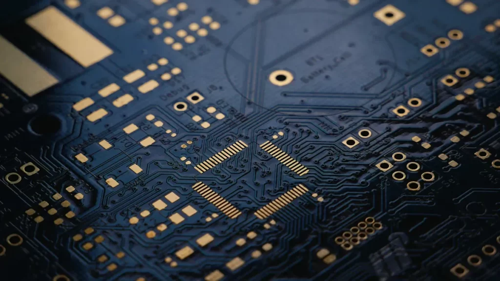

The need for modern gadgets drives progress in consumer electronics PCBA manufacturing and circuit boards. Tools like Surface Mount Technology and Automated Optical Inspection are key in this process. The global PCB market was worth $68.4 billion in 2023 and is expected to grow to $105.8 billion by 2032, rising 4.9% yearly. These technologies help make devices smaller, quicker, and better. Making electronics depends on these advanced methods for accuracy and trust.
Key Takeaways
Surface Mount Technology (SMT) makes PCB assembly better. It uses smaller, lighter parts placed on the board’s surface. This saves money and works faster.
Automated Optical Inspection (AOI) checks PCBs for mistakes quickly. It helps save time, lowers costs, and keeps customers happy.
Industry 4.0 tools like IoT and AI help PCB making. They allow real-time checks and fix problems early, making work faster with less waiting.
High-Density Interconnect (HDI) technology helps create smaller, smarter PCBs. It is important for modern gadgets that need to work well in tiny spaces.
Flexible and rigid-flex PCBs are great for creative designs. They help make smaller, stronger devices that fit different shapes and uses.
Surface Mount Technology (SMT) in PCB Assembly
Role of SMT in consumer electronics PCBA manufacturing
Surface Mount Technology (SMT) is very important in making PCBs for consumer electronics. It lets parts stick directly to the board’s surface, skipping older through-hole methods. This change has improved how PCBs are built and designed. For instance, SMT helps create small and light gadgets like IoT wearables and smart home systems. These devices use layered PCBs with surface-mounted parts for better assembly and dependability.
SMT has come a long way over time. It started in the 1960s when IBM used it for the Launch Vehicle Digital Computer. By 1986, 10% of the market used surface-mounted parts. By the late 1990s, SMT became the main method for advanced PCB assemblies.
Year | Key Milestone |
|---|---|
1960s | Surface Mount Technology (SMT) was first developed. |
1986 | 10% of the market used surface-mounted parts. |
Late 1990s | SMT became the top choice for advanced PCB assemblies. |
1960 | IBM used SMT for the Launch Vehicle Digital Computer. |
Benefits of SMT for miniaturization and efficiency
SMT has changed PCB design by making layouts smaller and more efficient. It allows more parts to fit on the board because they attach directly to the surface. This is crucial for modern gadgets, where being small is key. Automated machines used with SMT also make production faster and cheaper.
Features | SMT | Through-Hole Technology (THT) |
|---|---|---|
Component size | Smaller and compact | Larger components |
Assembly process | Automated with pick-and-place machines | Manual or semi-automated |
Cost | Lower overall cost | Higher cost due to labor-intensive process |
PCB density | Higher density possible | Limited due to larger components |
With SMT, parts are smaller and lighter, assembly is quicker, and costs are lower. These benefits make SMT the top choice for making consumer electronics.
Impact of SMT on modern PCB manufacturing processes
SMT has greatly improved how PCBs are made today. It cuts costs by saving board space and allows automated assembly. This makes it perfect for making large quantities. SMT also removes the need for drilling, making production simpler.
In consumer electronics, SMT helps create small designs, pack more parts, and add more features. For example, car electronics use SMT for reliable ECUs and infotainment systems. Medical devices like pacemakers also use SMT to stay small and dependable.
Sector | How SMT Helps |
|---|---|
Consumer Electronics | Makes devices smaller, adds more parts, and boosts features. |
Automotive Electronics | Ensures reliable ECUs, infotainment systems, and safety features like ADAS. |
Medical Devices | Keeps devices like pacemakers small and reliable. |
Industrial Equipment | Improves how robots and automation systems work. |
Telecommunications | Supports dense, reliable networking tools for modern communication. |
Using SMT means better efficiency, accuracy, and scalability in PCB making. This technology keeps pushing consumer electronics forward.
Automated Optical Inspection (AOI) for Quality Assurance
How AOI improves defect detection in PCB assembly
Automated Optical Inspection (AOI) helps ensure PCBs are made correctly. It uses cameras and imaging tools to find mistakes quickly. AOI spots problems like bad soldering, misplaced parts, or surface damage. By catching these issues early, it stops faulty boards from moving forward. This saves both time and money.
Defect Type | What AOI Detects |
|---|---|
Soldering defects | Too much, too little, or bridged solder |
Component misalignment | Wrong placement or missing parts |
Physical defects | Scratches, cracks, or dirt on the board |
Early fault detection | Finds errors before the next production step |
High inspection speed | Checks boards fast, improving production speed |
Consistent quality control | Reliable checks without human mistakes |
AOI also works very fast, helping factories produce more PCBs. It keeps production smooth while making sure quality stays high.
Benefits of AOI for reliability in consumer electronics
AOI makes sure only good PCBs are used in devices. It is 95% effective at finding problems, making it very reliable. This lowers the chance of broken gadgets reaching customers, keeping them happy.
Evidence Type | Details |
|---|---|
Effectiveness Rate | AOI finds 95% of defects, proving its reliability. |
Cost of False Detections | Mistakes cost about $7000 per panel each year. |
Unplanned Downtime | 82% of factories lose time due to unexpected problems. |
By reducing errors and downtime, AOI keeps production cheaper and smoother. This helps electronics brands maintain a good reputation.
Impact of AOI on reducing production costs and errors
AOI lowers costs by finding mistakes early in the process. Fixing problems later is expensive, so early detection saves money. It also makes production faster and more efficient.
Evidence Type | Details |
|---|---|
Quality Control | AOI catches mistakes early, saving money and improving efficiency. |
Cost Effectiveness | AOI is cheaper than other methods and prevents repeated errors. |
Process Improvement | Early problem detection helps find patterns and avoid future issues. |
For example, one big electronics company saved $2 million yearly and cut defects by 40% using AOI. A smaller company reduced inspection time by 60%, allowing them to handle harder designs and satisfy customers better.
Adding AOI to your process improves quality, reduces mistakes, and cuts costs. It is a must-have for modern PCB manufacturing.
Industry 4.0 and Smart PCB Manufacturing
How IoT and AI improve PCB manufacturing
IoT and AI have made PCB manufacturing smarter and faster. IoT sensors in machines check performance all the time. They find problems early, so repairs can be planned ahead. This saves time and money. For example:
Sensors on pumps notice wear and stop sudden breakdowns.
Predictive maintenance uses data to keep machines working longer.
AI makes automation better by studying production data instantly. It spots patterns, fixes workflows, and keeps quality steady. Together, IoT and AI make manufacturing smooth and ready for consumer electronics.
Why real-time monitoring and predictive analytics matter
Real-time monitoring and predictive analytics help catch problems early. Watching machines and processes closely avoids costly delays. Predictive analytics uses data to guess issues and fix them in time.
Benefit | Percentage Improvement |
|---|---|
Less machine downtime | 30–50% |
Higher production rates | 10–30% |
Better worker productivity | 15–30% |
Smarter demand predictions | 85% |
These tools make manufacturing more efficient. Predictive maintenance stops surprise breakdowns. AI checks for defects early, ensuring high-quality PCBs. This boosts the reliability of electronics.
How Industry 4.0 changes PCBA scalability and customization
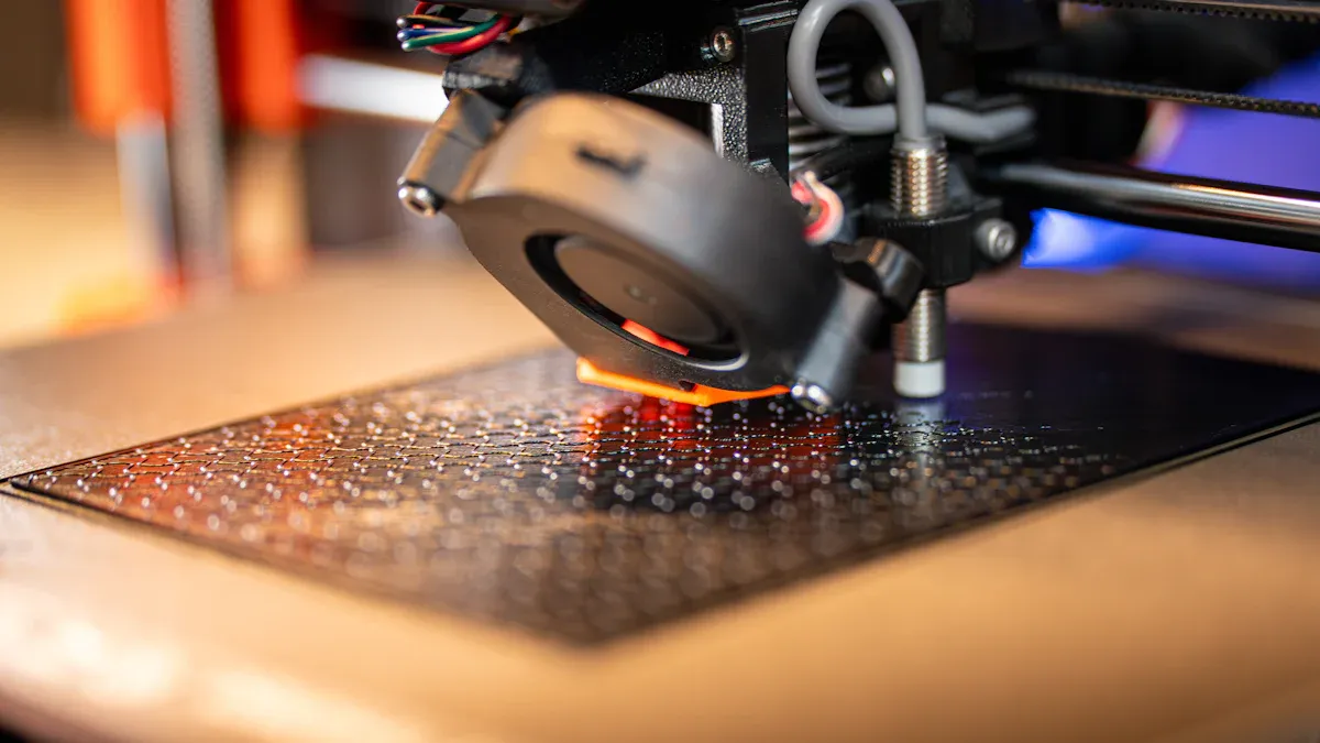
Industry 4.0 has changed PCB manufacturing by adding flexibility and growth. New tech like 3D printing helps create detailed designs fast. This is important for meeting different customer needs.
Smart manufacturing also improves how data is handled. Using the “5Vs” (Volume, Velocity, Variety, Veracity, and Value), data is studied better. This helps make smarter choices and flexible production lines. Manufacturers can now grow and customize PCBs to fit specific needs. This keeps them ahead in a fast-changing market.
High-Density Interconnect (HDI) Technology
Role of HDI in compact and complex PCB designs
High-Density Interconnect (HDI) helps make small and detailed PCBs. Modern gadgets like phones and smartwatches use HDI PCBs to fit more parts in tiny spaces. These boards have very thin circuits, less than 0.005 inches wide. This saves space and makes the board more efficient.
HDI PCBs connect layers using special vias like blind, buried, and stacked ones. Microvias, smaller than 0.008 inches, allow tricky paths without making the board bigger. Making HDI PCBs involves steps like laser drilling, plating, and layering. New tools, like pulse-spray systems and laser-drilled vias, improve how precise and strong these boards are.
Tip: HDI PCBs are great for designing small, high-quality electronics.
Benefits of HDI for high-performance consumer electronics
HDI PCBs have many perks for advanced electronics. They pack more parts into smaller devices, adding more features. For example, HDI boards can have up to 50 layers, while regular ones usually have 12. This makes them perfect for gadgets like 5G phones and medical tools.
Feature | HDI PCBs | Standard PCBs |
|---|---|---|
Component Density | Fits more parts | Fits fewer parts |
Line/Space | 25-50 micron lines/spaces | ~100 micron lines/spaces |
Number of Routing Layers | Up to 20-50 layers | Usually ≤ 12 layers |
Materials | Special high-speed materials | Regular FR-4 materials |
Vias | Tiny microvias (<100 micron) | Bigger plated holes (≥ 150 micron) |
HDI PCBs improve signals, speed up data, and handle heat better. These features make HDI a key part of making modern electronics.
Impact of HDI on the future of PCB manufacturing
HDI will shape how PCBs are made in the future. The PCB market is expected to grow from $70 billion in 2023 to $85 billion by 2025. This growth comes from better telecom, car electronics, and medical devices. HDI PCBs are important because they meet the need for smaller and faster gadgets.
Year | Market Size (USD Bn) | CAGR (%) |
|---|---|---|
2024 | 16.11 | N/A |
2032 | 39.91 | 12 |
HDI will lead the way with new tech like AI design tools and eco-friendly materials. These upgrades will make HDI PCB production even better. HDI will stay a top choice for making advanced consumer electronics.
Flexible and Rigid-Flex PCBs in Consumer Electronics
Uses of flexible PCBs in today’s gadgets
Flexible PCBs are important for modern electronics. They fit into small spaces and adjust to different shapes. You can see them in foldable phones, tablets, and wearables. These devices need flexible PCBs to work well while bending or changing shape.
The need for flexible PCBs is growing because they are light and save space. They are perfect for slim gadgets like smartwatches and fitness bands. Flexible PCBs also work in devices with tricky shapes, like medical tools and car electronics. They handle movement well, making them dependable for moving parts.
Advantages of rigid-flex PCBs for strength and flexibility
Rigid-flex PCBs mix the toughness of rigid boards with the flexibility of flexible ones. They are great for places with lots of shocks or vibrations. These PCBs can bend many times without breaking, lasting a long time.
Their design has fewer connection points, which improves signals and reduces interference. This also means fewer steps to assemble, saving money. Rigid-flex PCBs are strong but light, making them good for aerospace systems and portable medical tools. They stay reliable even in tough conditions.
How flexible PCBs help make smaller devices
Flexible PCBs are key to building small and efficient gadgets. They bend and fit into tight spaces, perfect for phones and wearables. These PCBs are thinner and lighter than rigid ones, ideal for portable devices.
Their design allows more parts to fit in less space, cutting down on extra components. For example, in phones, flexible PCBs link screens and sensors, saving room inside. In wearables, they match body shapes, improving comfort and use. Flexible PCBs also ensure safe and steady connections in car electronics, even in tough conditions.
Consumer electronics PCBA manufacturing uses new ideas like SMT, AOI, Industry 4.0, HDI, and flexible PCBs. These tools help make devices smaller, faster, and more dependable. AI and IoT make assembly better with real-time checks and smart predictions. Better materials and machines make PCB production more accurate. In the future, smarter systems like digital twins and AI-designed PCBs will keep improving things. The industry is also focusing on being eco-friendly, using green materials and saving energy. These changes promise exciting growth for electronics and PCB making.
FAQ
What is PCB assembly, and why does it matter?
PCB assembly means putting electronic parts on a circuit board. It makes sure devices work by connecting parts properly. This step is key for making today’s electronics.
How is SMT different from older PCB methods?
SMT puts parts right on the board’s surface. Older ways needed holes drilled into the board. SMT makes devices smaller, faster to build, and cheaper to produce.
Can flexible PCBs make devices last longer?
Yes, flexible PCBs handle movement better and lower stress on parts. They are perfect for gadgets like wearables and car electronics that need to bend and stay strong.
Why is AOI important in PCB assembly?
AOI checks for mistakes early during assembly. It uses cameras to find problems like misplaced parts or bad soldering. This saves time and cuts costs.
How does Industry 4.0 change PCB manufacturing?
Industry 4.0 uses IoT and AI to watch and fix machines in real-time. It helps factories work faster, avoid delays, and make custom PCB designs easily.
See Also
Discover The Role Of AI In PCBA For Electronics
Essential Techniques For Achieving Quality In PCBA Manufacturing
Comparing Turnkey And Consignment PCBA Manufacturing In 2025