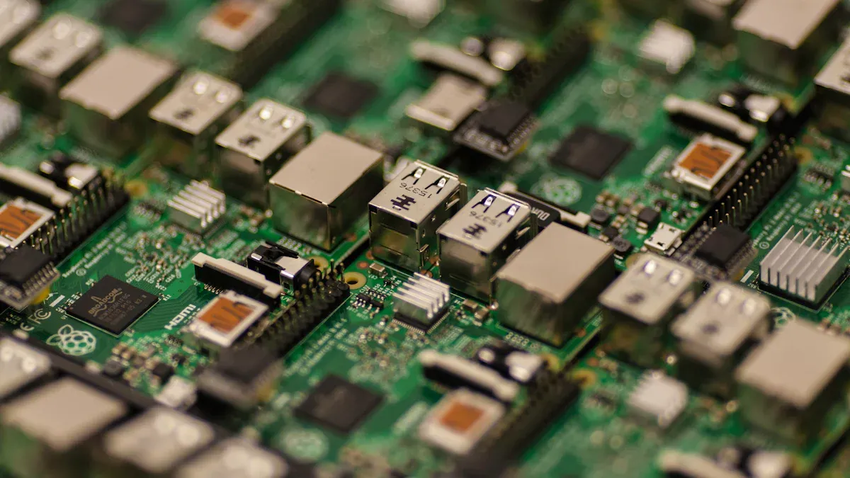
Designing circuit boards for low power industrial IoT PCB design and assembly requires care and creativity. Focus on creating low-power IoT PCBs to enhance efficiency and reliability. Industrial spaces present unique challenges such as power conservation, durability, and compactness. Effective PCB design plays a crucial role in optimizing low-power devices. By addressing these challenges, you can develop devices that last longer, consume less energy, and meet the demands of modern IoT applications.
Key Takeaways
Use power-saving methods like lowering voltage and sleep modes to save energy in IoT devices.
Pick energy-efficient parts, like SiC MOSFETs, to reduce energy waste and improve low-power PCB performance.
Design small layouts, like HDI PCBs, to save space and handle heat better in industrial areas.
Test carefully with in-circuit and stress tests to make sure your PCB works well and meets industry rules.
Work together with different engineers to share ideas and create smart low-power PCB designs.
Understanding Low-Power Design Principles
Power management strategies for industrial IoT
Managing power well helps IoT devices use less energy. This also keeps them working efficiently. One way is dynamic voltage scaling. It changes the voltage based on the device’s work. This saves energy when the device is idle. Another method is using sleep modes. Parts not in use go into a low-energy state. For instance, sensors can stay off until needed.
Power-gating is another helpful method. It cuts power to parts not being used. This lowers energy use even more. Using these methods together helps balance performance and energy saving. These strategies are great for devices that need to work long without much maintenance.
Energy-efficient architecture and optimization
Building PCBs with energy-saving designs helps IoT devices work better. They also use less power. One smart method is combining the LEACH protocol with digital twin technology. Studies show this reduces non-working parts by 83%. It also boosts energy levels by 1.66 times compared to older ways. This proves how advanced methods can save energy.
When designing PCBs, reduce signal loss and heat. Multi-layer PCBs help lower resistance and improve connections. Also, think about 5G-enabled IoT. It sends data faster and uses less energy for communication. By focusing on these ideas, you can make systems that save power but still work well.
Selecting components for low power devices
Picking the right parts is key to saving energy in IoT devices. Silicon carbide (SiC) parts are better than regular silicon ones. SiC MOSFETs with SiC diodes work best at different frequencies. They have the least energy loss when switching or conducting. This makes them perfect for low-power IoT PCB designs.
Component Type | Efficiency at 20 kHz | Efficiency at 50 kHz | Conduction Loss | Switching Loss |
|---|---|---|---|---|
Si MOSFET + SiC diode | 97.8% | Lower | Higher | Moderate |
SiC MOSFET + SiC diode | Best | Even lower | Lowest | Lowest |
Si IGBT + SiC diode | Lower | Even lower | Highest | Moderate |
Besides saving energy, parts should last long and be reliable. Easy-to-replace parts, like sensors, make fixing problems simpler. This keeps the system running smoothly. It also makes IoT devices stronger for tough industrial jobs.
Key Design Considerations for Low Power Industrial IoT PCB Design and Assembly
Power optimization techniques (e.g., sleep modes, power-gating)
Saving energy is important for industrial IoT devices. Sleep modes let parts use less power when not working. For example, special microcontrollers can stay in sleep mode to save battery. This helps devices work longer, even in faraway places.
Power-gating is another way to save energy. It turns off parts of the circuit not being used. When needed, these parts turn back on. This reduces wasted energy while keeping the device working well. Power-gating also checks circuits for problems using Iddq testing. By using both sleep modes and power-gating, devices can save energy and still work reliably.
Technique | Description | Results |
|---|---|---|
Energy harvesting | Collects energy from vibrations | Works for 5+ years without maintenance |
Ultra-low-power MCU | Uses sleep mode to save energy | No need for battery changes |
Optimized data compression | Sends data more efficiently |
Material selection for durability and efficiency
Picking the right materials makes PCBs last longer and work better. Materials like CF-004 handle heat better than FR-4. They have higher glass transition temperatures (Tg) and lower thermal expansion (CTE). This means they won’t break apart in hot conditions, making them great for tough jobs.
CF-004 also helps with electrical performance. It has a dielectric constant (Dk) between 4.2 and 4.7, which is good for fast circuits. It loses less energy and provides better insulation, even in wet places. Choosing materials like CF-004 improves how long IoT devices last and how well they work.
Thermal Stability:
Glass Transition Temperature (Tg): CF-004 handles heat better than FR-4.
Coefficient of Thermal Expansion (CTE): CF-004 expands less, making it stronger.
Delamination Resistance: CF-004 avoids breaking in high heat.
Electrical Performance:
Dielectric Constant (Dk): CF-004 supports fast circuits better than FR-4.
Dissipation Factor (Df): CF-004 wastes less energy.
Insulation Resistance: CF-004 works well in wet conditions.
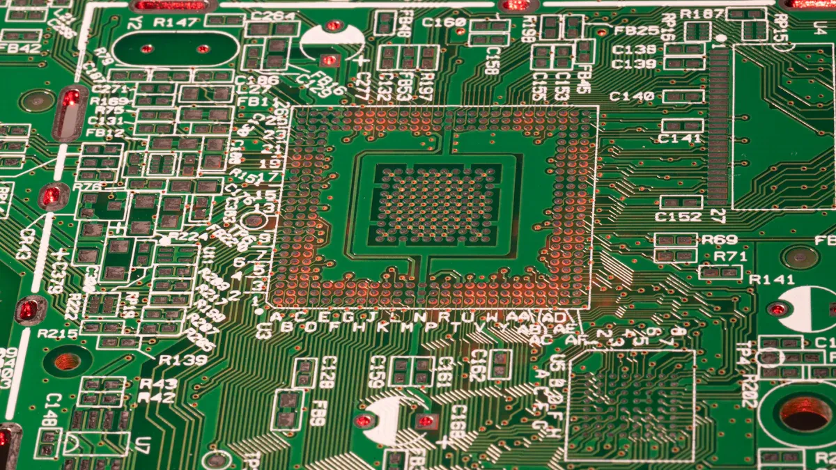
Compact layout design for industrial environments
Small designs are important for IoT devices in tight spaces. HDI PCBs help fit more parts into smaller areas. This keeps devices small but still working well.
Placing parts smartly and using multi-layer designs make PCBs even smaller. These ideas improve connections and reduce signal problems. Good thermal management is also key. It stops devices from overheating, so they work better. By focusing on small designs, IoT devices can handle the needs of modern industries.
Small PCB designs are needed for tight spaces in industries.
HDI PCBs fit more parts into smaller areas without losing quality.
Smart layouts and multi-layer designs make PCBs smaller and better.
Keeping devices cool is important for good performance.
Compact designs help IoT devices work well in real-world conditions.
Prototyping and Testing for Power Consumption Optimization
Iterative prototyping and validation
Making prototypes is key to improving your IoT PCB design. Build and test different versions to find and fix problems early. Start by checking the design with your team to catch mistakes. Regular team reviews help ensure nothing is missed. Use version control to keep track of changes and avoid mix-ups. Feedback from testing should guide you in making the design better.
Each version may need changes to parts placement, wiring, or layers. After updating, create a new prototype to test the fixes. Keep improving until the design meets all needs. Then, finalize it for large-scale production. This step-by-step process ensures your PCB uses less power and works efficiently.
Best Practice | Description |
|---|---|
Review | Check the design often with your team to find issues. |
Version Control | Keep track of changes to avoid mistakes. |
Feedback Integration | Use test results to make the design better. |
Testing for power consumption and efficiency
Testing makes sure your IoT device works well and saves energy. Start by measuring how much power each part uses in different situations. This helps you find where energy can be saved. Use tools like multimeters and oscilloscopes to check voltage and current levels.
Energy-saving devices often use low-power microcontrollers and smart data transfer. Test these parts to see if they meet performance goals. Also, try out different working conditions to see how the PCB handles power in real life. These tests help you adjust the design for the best energy use.
Real-world condition testing and compliance
Testing in real-world conditions ensures your IoT PCB works in tough environments. Simulate extreme heat, cold, and vibrations to check its strength. Environmental stress testing (EST) shows if the PCB can handle harsh conditions.
In-circuit testing (ICT) checks if all electrical parts are connected properly. Functional testing (FT) makes sure the PCB works as it should. These tests confirm your design meets industry rules and standards. Careful testing helps you create a strong and energy-efficient PCB for 5G IoT devices.
Testing Method | Purpose |
|---|---|
In-Circuit Testing (ICT) | Checks if all parts are connected correctly. |
Functional Testing (FT) | Makes sure the PCB works as planned. |
Environmental Stress Testing (EST) | Tests if the PCB can handle tough conditions. |
Tip: Always write down test results and compliance details. This helps track performance and proves your design meets industry rules.
Challenges and Tradeoffs in Low Power PCB Design
Balancing battery life and performance
Making devices last long on batteries is a big challenge. You must save energy while keeping the device working well. For battery-powered devices, managing energy use is very important. Using sleep modes and lowering sleep current can help batteries last longer. For example, special microcontrollers use very little power when not active. But, improving performance can use more energy, which shortens battery life.
To solve this, use power-saving methods that match your device’s needs. For 5G IoT devices, smart data transfer can save energy while staying connected. Picking the right parts and designing carefully can balance good performance with long battery life.
Managing cost vs. power efficiency
Saving money and saving energy can be hard to balance. Using fewer layers or cheaper materials lowers costs but may waste more energy. A simpler design can cost less to make but might not save as much power. Choosing common materials instead of expensive ones can save money while still working well.
To handle this, try these steps:
Pick low-power parts that fit your budget and needs.
Design the PCB to save money without losing quality.
Work with suppliers early to get good prices and parts.
Reuse designs to save time and cut costs.
By doing this, you can make a design that saves both money and energy.
Addressing interoperability and industrial protocol requirements
IoT devices need to work well with other systems. Supporting common protocols like MQTT and OPC UA helps devices communicate easily. For low-power designs, plan carefully to include these protocols. Using switching regulators and energy harvesting can save energy while staying compatible.
Protocols like ICP/CFX make data sharing easier and use less power. PCBs connect parts like sensors and processors, helping systems work automatically. By focusing on compatibility, your design can work in many places and still save energy.
Best Practices for Low Power Industrial IoT PCB Design
Working Together Across Teams
Teamwork is important for making low-power PCBs. Bring in experts from different areas like electrical, mechanical, and software engineering. Each team helps improve the design in unique ways. Electrical engineers can handle power use, while software engineers make programs that save energy.
Here are some teamwork success stories:
Project Description | Application | Key Achievements |
|---|---|---|
Low-noise detector board for neutron detection | Ionization-mode thermal neutron detector | Achieved high detector rates (up to 106 neutrons/sec) |
Low-noise ASIC carrier board for gamma-ray detection | Virtual Frisch-grid CZT gamma-ray detectors | Used by U.S. Department of Energy for advanced detection tasks |
These examples show how teamwork leads to smart solutions for industrial IoT.
Learning from Consumer IoT for Industry
Consumer IoT devices often have great new ideas. You can use these ideas for industrial designs. For example, small designs and energy-saving microcontrollers from consumer devices can inspire industrial PCBs. Features like better data compression and low-energy wireless tools are useful too.
By watching consumer IoT trends, you can find ways to save battery and lower energy use. For instance, using ultra-low-power sensors from consumer devices can make industrial systems work better. This method combines consumer and industrial needs, keeping your designs modern.
Following Industrial Rules and Standards
Following rules is very important for IoT devices. Your PCB must work with protocols like MQTT, OPC UA, and Modbus. These help devices talk to each other in factories. Meeting standards also makes devices reliable and easy to use with other systems.
Testing helps ensure your design follows the rules. Use in-circuit testing (ICT) to check connections and functional testing (FT) to see if the PCB works right. Environmental stress testing (EST) checks if the device can handle tough conditions. By focusing on these tests, you can make strong and reliable IoT devices.
Creating low-power PCBs for industrial IoT is very important. It helps save energy, makes devices last longer, and keeps them small. Using smart energy-saving ideas can make batteries last longer. It also helps devices work better in tough places.
You need to think about everything when designing PCBs. This includes technical needs, the environment, and how the device will be used. Trying new ideas and following good practices can lower power use. This improves how devices work and helps them last longer. Start using these tips now to build smarter and more efficient devices.
FAQ
How can IoT devices have longer battery life?
Use parts that need less power. Add sleep modes to save energy when the device is not working. Send data in smarter ways to use less energy. These steps help devices work longer without needing new batteries.
What materials make a PCB strong and long-lasting?
Pick materials that handle heat well and don’t expand much. For example, CF-004 is better than FR-4. It resists heat and works better for electricity, making it great for tough industrial jobs.
Why are small PCB designs important for industrial IoT?
Small designs fit into tight spaces and work better in factories. HDI PCBs and multi-layer layouts let you add more parts in less space. This keeps the device small but still powerful.
How does power-gating save energy?
Power-gating turns off parts of the circuit not being used. This stops energy waste while keeping the device working well. It’s a smart way to save power in IoT devices.
What tests check if a PCB meets industry rules?
Tests like ICT, FT, and EST check if the PCB works right. They also test if it can handle tough conditions. These tests make sure the PCB follows rules and works reliably.
See Also
Creating IIoT Sensor Node PCBAs for 2025 Manufacturing
Enhancing Industrial Automation Efficiency Through PCBA Solutions
The Importance of PCBA Manufacturing for IoT Devices Today
Evaluating Features of Industrial IoT Gateway PCB Assemblies