
Smart Manufacturing PCBA is changing how things are made. New tech like AI, IoT, and robots make work faster. For example, car PCBs may grow 6.9% in 2025 due to self-driving cars. Also, energy use in making chips might grow 12% yearly from 2025 to 2035. These changes show why eco-friendly ideas and new tools are important. Keeping up with these changes helps you stay competitive and prepared for the future.
Key Takeaways
Use AI and machines to make PCB production faster and more accurate. This saves money and boosts efficiency.
Add IoT tools to build smart factories. Watching processes live can cut delays and keep quality high.
Choose strong materials like polyimide and PTFE for better PCBs. These materials last longer and work well for 5G signals.
Follow eco-friendly methods to use less energy and create less waste. Helping the planet can also attract green-minded buyers.
Learn about smaller designs and HDI technology. These ideas help make tiny electronics that fit modern needs.
Advancements in AI and Automation
AI-driven process optimization
AI is changing how pcbs are made by improving every step. It helps designs become more accurate, speeds up production, and saves money. For example, AI finds defects faster, cutting mistakes and boosting efficiency. The table below shows how AI makes manufacturing better:
Benefit Type | Description |
|---|---|
Better Accuracy | AI finds defects quickly, lowering mistakes a lot. |
Faster Production | AI makes production lines quicker, saving time. |
Cost Savings | Finding problems early reduces waste and saves money. |
Using AI can make automated production smoother and help you stay ahead in pcb manufacturing.
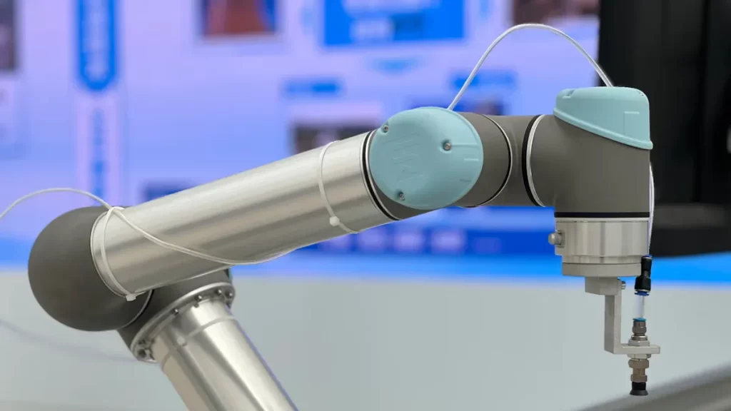
Robotics in PCB assembly and inspection
Robots are important for making and checking pcbs. They work with great accuracy, reduce mistakes, and cut labor costs. For example, robots have lowered defects by 35% and shortened production times by 25%. Now, 60% of pcb factories use robots, and they see profits in just 18 months.
Robots ensure high quality, especially in tiny electronics, where accuracy is over 90%. Adding robots can make production faster and meet the need for better pcbs.
Benefits and challenges of AI in smart manufacturing pcba
AI and automation bring many good changes to pcb manufacturing. They find defects better, make processes steady, and save inspection time. For example, automated optical inspection (AOI) has replaced manual checks. This change cut errors by 94% and inspection time by 82.5%. These tools handle complex pcbs while improving production.
But there are challenges too. Using AI in supply chains costs a lot and needs skilled workers. Also, connecting AI to old systems can be tricky. Even with these issues, the benefits of AI and automation are huge. That’s why they are a big trend in pcb manufacturing.
Integration of IoT and Smart Technologies
IoT-enabled smart factories
IoT is turning regular factories into smart ones. These factories use connected devices to work better and faster. For example, IoT sensors check machines to keep them running well. They look at data instantly to find and fix problems fast. This reduces downtime and keeps production smooth. It also helps make high-quality pcbs every time.
More factories are using IoT technology. In 2023, over 63 million US homes had smart devices. By 2027, this number might reach 93 million. This shows how important IoT is becoming. Manufacturers now need to use smart tools to stay ahead in pcb production.
Real-time monitoring and predictive maintenance
Real-time monitoring is key in making pcbs today. Smart systems like DeepSeek watch machines all the time. They check parts and supply chains to spot risks early, like running out of stock. Warnings help fix problems before they cause delays.
Predictive maintenance makes things even better. It tells when machines need fixing, avoiding sudden breakdowns. This keeps machines working longer and reduces downtime. Real-time monitoring also catches problems quickly, lowering defects. These tools make production smoother and pcbs better.
Benefits and challenges of the integration of AI and IoT in pcb manufacturing
AI and IoT bring many benefits to pcb production. AI speeds up inspections and makes them more accurate. Predictive maintenance cuts downtime, and constant monitoring keeps quality steady. AI also saves money by finding waste and fixing it.
But there are some challenges too. Skilled workers are needed to handle these systems. Old inspection methods can slow things down, and process changes might cause mistakes. Even with these issues, AI and IoT are still top trends. They help make pcb production faster and smarter.
Use of Advanced Materials
High-performance substrates and conductive materials
New materials are changing how pcbs are made. Polyimide is one example. It handles heat well and bends easily. This makes it great for cars and airplanes. It works better than older materials like FR-4, which struggle with heat and signals. For instance, polyimide stays strong in very hot or cold places, making it reliable.
For fast signals, the dielectric constant is important. Materials like PTFE have a low dielectric constant of 2.1. This helps signals move faster, perfect for 5G devices. On the other hand, materials with high dielectric constants slow signals down. PTFE and polyimide also reduce signal loss, which is key for fast circuits. These materials make pcbs work better and last longer in advanced tech.
Flexible and stretchable PCBs
Flexible and stretchable pcbs are changing designs in smart manufacturing. They cut wiring mistakes and remove the need for connectors. They also allow more circuits in smaller spaces. This makes them perfect for tiny, lightweight gadgets.
But flexible pcbs have some issues. They cost more and can break easily. Careful handling is needed to avoid scratches or damage. For example, bad storage can ruin them. The table below shows the pros and cons of flexible pcbs:
Advantages of Flexible PCBs | Disadvantages of Flexible PCBs |
|---|---|
Fewer wiring mistakes | Higher material costs |
No need for connectors | Low heat resistance |
Easier to design | Harder to assemble |
More circuits in small spaces | Easy to damage |
Better signal quality | Scratches easily |
More reliable | Hard to fix if broken |
Smaller and lighter | Needs special storage |
Flexible pcbs open new possibilities but need careful handling during production.
Benefits and challenges of advanced materials in pcb manufacturing
Advanced materials bring many benefits to pcb making. They lower costs, improve quality, and boost performance by reducing signal problems. For example, eco-friendly methods meet rules and help the environment.
However, there are challenges too. New tools and materials cost a lot upfront. Planning is needed to balance costs and future savings. Keeping quality high with advanced methods also takes effort. The table below sums up these points:
Benefit/Challenge | Description |
|---|---|
Lower Costs | Advanced materials can make pcb production cheaper. |
Better Quality | New materials make pcbs stronger and last longer. |
Improved Performance | They reduce signal problems, making pcbs work better. |
Eco-friendly Methods | Green processes meet rules and protect the environment. |
High Starting Costs | New tools and materials need big upfront spending. |
Cost Balancing | Managing costs and savings over time is tricky. |
Quality Control | Keeping quality high with new methods is challenging. |
Using advanced materials helps pcb makers stay ahead, but they must handle challenges wisely.
Sustainability and Green Manufacturing
Eco-friendly materials and processes
Making pcbs in a greener way is becoming popular. Factories now use materials like lead-free and eco-friendly substrates. These materials follow environmental rules and make recycling easier.
To cut waste, factories are improving how they work. They skip extra steps, like using low-temperature soldering and dry etching. Experts think 20% of pcbs will be made sustainably by 2033. Big companies like Samsung and Apple are already using green methods to save money and help the planet.
Energy-efficient manufacturing techniques
New ways to save energy are changing how pcbs are made. Modern machines use less power but work 30% faster. Robots and automation also help by cutting costs and speeding up production.
Factories now use things like low-temperature soldering and renewable energy. These changes lower pollution and save energy. Recycling and using fewer materials also help meet strict green rules. These methods save money and attract eco-friendly investors.
Benefits and challenges of sustainable pcb manufacturing
Green practices bring many good changes to pcb making. Recycling and less waste save money and help the earth. Using less energy makes production faster and cleaner. Eco-friendly soldering meets green rules.
But there are problems too. Starting with green tech can cost a lot. Skilled workers are needed to run these systems. Even with these issues, going green is key for long-term success.
Benefits of Sustainable Practices | Challenges of Sustainable Practices |
|---|---|
Recycling and Waste Reduction | High starting costs |
Energy-Efficient Manufacturing | Need for skilled workers |
Eco-Friendly Soldering Techniques |
Using green methods helps you stay ahead and protect the planet.
Miniaturization and High-Density Interconnects
Trends in miniaturized components and HDI PCBs
Smaller, stronger gadgets need tiny parts and HDI PCBs. These let more features fit into small spaces. They are great for phones, wearables, and medical tools. HDI technology helps by creating detailed circuits and tight connections.
Key Trends in Miniaturization and HDI PCBs | Description |
|---|---|
Shrinking PCB Sizes | Smaller PCBs fit compact devices better. |
Increased Component Density | HDI technology adds more parts in less space. |
Enhanced Signal Integrity | New materials improve signals and reduce loss. |
Application in Diverse Industries | Used in electronics, planes, and medical tools. |
Miniaturization also happens in chips, making PCBs smaller. This keeps gadgets light but still powerful.
Benefits and challenges of compact designs in pcb manufacturing
Tiny designs have many perks. They make gadgets lighter and easier to carry. More parts in small spaces boost features. Microvias improve signals and cut interference. These are key for top PCBs in healthcare and aerospace.
But tiny designs are tricky. Making small PCBs needs special tools and skills. Microvias and layers can cost more to produce. Also, dense circuits must handle heat well to avoid damage.
Tip: Use HDI technology and modern tools to solve these issues and stay ahead.
By using miniaturization and HDI PCBs, you can create sleek, high-tech gadgets. These trends keep your products smart and efficient.
5G and High-Frequency PCB Technologies
Requirements for 5G-enabled PCBs
5G needs advanced PCBs to work well. These PCBs must handle high frequencies, fast data, and keep signals clear.
The table below shows key features for different 5G uses:
5G Service | Frequency Range | Key Performance Metric | Example Applications |
|---|---|---|---|
Enhanced Mobile Broadband (eMBB) | Sub‑6 GHz, 24 – 50 GHz mmWave | 10 Gbps peak downlink | 8K video streaming, AR/VR |
Ultra‑Reliable Low‑Latency Communications (URLLC) | Sub‑6 GHz | <1 ms end‑to‑end latency | Autonomous driving, remote surgery |
Massive Machine‑Type Communications (mMTC) | Sub‑1 GHz, 3 – 5 GHz | 1 M devices/km² | Smart cities, IoT sensors |
To meet these needs, PCBs must use materials and designs that reduce signal loss and handle high frequencies.
High-frequency materials and designs
Special materials like PTFE and ceramic laminates are used for 5G PCBs. These materials keep signals fast and steady. For example, PTFE works well in 5G because it handles heat and reduces signal loss.
5G PCB designs also need to fit advanced antennas and dense circuits. Smaller PCBs must hold more parts. Better heat control is needed to manage the heat from these tight circuits.
Benefits and challenges of 5G in pcb manufacturing
Adding 5G to PCB making has many benefits. It allows faster speeds, less delay, and better connections. For example, Huawei and China Mobile used 5G to help Haier process images quickly in automated factories.
But there are problems too. Handling heat and keeping performance high in small parts is hard. The table below lists the benefits and challenges:
Benefits | Challenges |
|---|---|
Enhanced speed | Managing extreme thermal conditions |
Lower latency | Ensuring high performance in smaller components |
Improved connection density | Necessitating advanced materials and techniques |
To stay ahead, factories need smart designs and automation for 5G-ready PCBs.
Emerging Applications in Key Industries
Automotive: Electric vehicles and autonomous systems
The car industry is changing with electric cars and self-driving systems. These new technologies need pcbs for GPS, ADAS, and electric engines. Multi-layer pcbs are in high demand because they handle complex systems well.
The rise of car electronics is changing the market. For example, the car pcb market might hit USD 17.08 billion by 2032. This growth comes from more advanced car electronics and stricter safety and pollution rules. Companies like BYD are leading with smart-car tech, showing how important innovation is in this field.
Evidence Type | Description |
|---|---|
Market Growth | Car pcb demand grows with EVs and ADAS. |
Market Segmentation | Modern cars need advanced pcbs for electronics. |
Regulatory Impact | Safety and pollution rules push advanced electronics use. |
Medical: Advanced diagnostic and wearable devices
Medical gadgets are getting smarter and smaller thanks to pcbs. Wearables like fitness trackers and health tools use tiny pcbs for accurate results. For example, the CircTrek device has a small pcb, just 42 mm x 35 mm. It includes parts like a narrow bandpass filter to improve signals and cut noise.
These changes are improving healthcare. Wearables now track health in real time, spotting problems early. Small pcbs also make portable health tools possible, helping people in faraway places. But making these tiny pcbs needs careful design and advanced methods to ensure they work well.
Aerospace: High-reliability PCBs for avionics and satellites
The aerospace field needs pcbs that survive tough conditions. Reliable pcbs are key for planes and satellites, where performance matters most. For instance, satellite systems need pcbs that handle signal issues and big temperature changes.
Case Study | Key Focus Areas |
|---|---|
Satellite Communication System | Design challenges, manufacturing innovations, and in-orbit performance data. |
Military Aircraft Upgrade Program | Obsolescence management, integration of new technologies, and certification processes. |
These pcbs are crucial for aerospace success. They power tech like navigation and communication systems. But making them is hard due to aging parts and strict rules. Using better materials and methods helps meet the high demands of this industry.
Benefits and challenges of industry-specific applications
PCBs are important in industries like cars, healthcare, and space. These industries gain a lot from advanced PCBs but face challenges too. Knowing these helps factories improve and stay ahead.
One big benefit is meeting strict rules. For example, car and airplane PCBs must follow rules like ISO9001 or IATF 16949. These rules ensure safety and good performance. But getting these certifications takes time and effort.
Another benefit is handling tough projects. Complex boards and flexible circuits are needed for electric cars, medical gadgets, and satellites. These designs show how far PCBs have come. However, they need special tools and skills, which can cost more.
Delivering on time is also very important. Industries like cars and healthcare need PCBs quickly to keep up with demand. Good processes help factories deliver on time. But weak systems can cause delays and problems.
Building strong client relationships is another plus. Happy clients return for more, showing trust in your work. This creates steady business. But keeping clients in a competitive market is hard. It needs new ideas and great service.
Factor | Benefits | Challenges |
|---|---|---|
Industry Rules and Standards | Proves quality and safety by following strict certifications. | Getting certifications like ISO9001 can be hard and slow. |
Handling Complex Projects | Shows skill in making advanced PCBs for special uses. | Needs costly tools and expert workers for complex designs. |
On-Time Delivery | Keeps production smooth by delivering PCBs as promised. | Delays happen if processes are not strong enough. |
Client Trust and Loyalty | Builds steady business through repeat customers. | Staying competitive needs constant improvement and great service. |
By learning these points, factories can improve their work. This helps them make better PCBs for different industries and meet their needs.
The main trends in PCB making for 2025 are changing things. HDI technology helps make smaller designs, and flexible PCBs improve wearables and IoT gadgets. Green methods lower harm to the environment, while automation makes work faster and products better. With 5G growing, high-frequency PCBs are more important than ever. These changes make production greener, improve how things work, and spark new ideas. Learning about these trends keeps you ready and competitive in smart PCB manufacturing.
FAQ
What is smart manufacturing in PCBA?
Smart manufacturing in PCBA uses new tech like AI, IoT, and robots. It makes PCBs faster, cheaper, and with fewer mistakes. This method also tracks machines in real time and predicts fixes to improve efficiency.
How does AI improve PCB manufacturing?
AI helps by finding problems, speeding up work, and cutting waste. It makes PCB assembly more accurate and reliable. For example, tools like automated optical inspection (AOI) spot errors quickly, saving time and money.
Why is IoT important in PCB production?
IoT links devices in factories to monitor them live. It finds problems early, reduces downtime, and keeps quality steady. IoT also uses data to make better decisions, improving how factories work.
What are the benefits of using advanced materials in PCBs?
Advanced materials make PCBs stronger, better with heat, and last longer. For example, materials like polyimide and PTFE handle high heat and fast signals. These materials are great for industries like 5G and aerospace.
How can green manufacturing benefit PCB production?
Green manufacturing cuts waste, saves energy, and follows eco-rules. Using eco-friendly materials and methods lowers costs and attracts green-minded clients. It also helps you stay ahead in a market that values the environment.
See Also
Key Developments Influencing Industrial IoT PCB Assembly By 2025
Essential Technologies Transforming PCBA Production For Today’s Electronics
Navigating ITAR Regulations For PCBA Production In 2025
Perfecting PCBA Production Methods For Superior Quality Outcomes
New Developments In FDA-Compliant PCBA Solutions For Healthcare